Since its launch, HaloFreeEtch has made significant progress toward its goal of enabling halogen-free, sustainable plasma etching processes for the semiconductor industry. The project’s first results demonstrate the feasibility of combining advanced modeling, experimental validation, and sustainability assessment into a single, integrated development framework.
computational screening & novel chemistries
Advancing Halogen-Free Etching Technologies
A major scientific outcome of HaloFreeEtch is the creation of a comprehensive database of halogen-free etchants, developed through advanced quantum chemical (DFT-based) computational screening. This approach allowed the consortium to evaluate the stability and reactivity of numerous candidate molecules and to identify a first set of promising halogen-free etching chemistries for further laboratory validation.
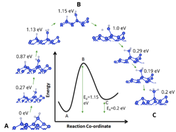
By integrating computational screening with process and plasma modeling, the project is significantly reducing experimental trial-and-error, accelerating the identification of viable alternatives to conventional halogen-based etching processes.
The modeling framework is designed to be extensible, allowing new chemistries and reactor geometries to be incorporated as kinetic data become available. This represents a key step beyond the state of the art and supports data-driven, sustainability-oriented process development.
integrated plasma, process & reactor modeling
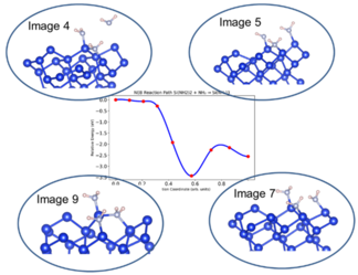
Multi-Scale Modeling for Sustainable Process Design
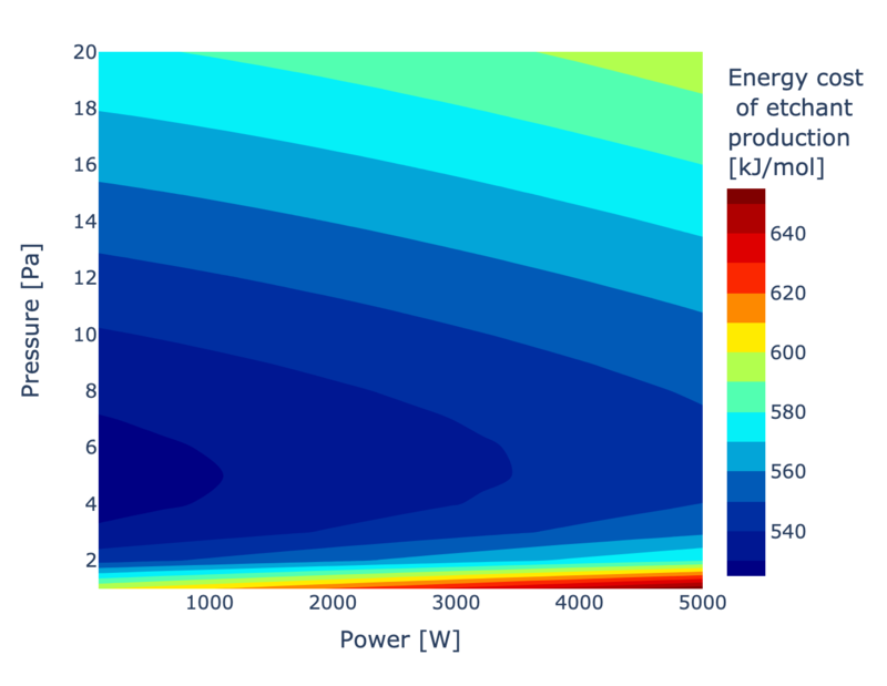
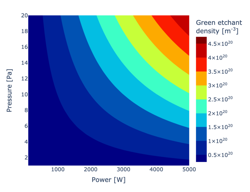
HaloFreeEtch has established a multi-scale modeling framework that links plasma chemistry, reactor-scale process behavior, and equipment-specific conditions. This framework has already been successfully applied to:
surface interactions & catalyst-assisted pathways
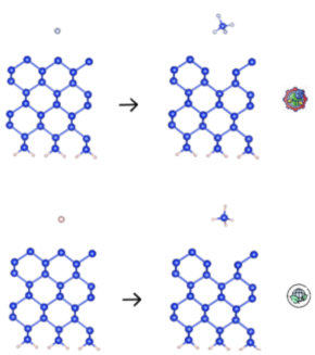
Experimental Validation and Catalyst-Based Etching
On the experimental side, first-year laboratory work focused on exploring catalyst-assisted silicon etching as a potential route toward halogen-free processes. Preliminary investigations included:
These foundational experiments establish the basis for future process optimization and scale-up activities planned in the next project phases.
To ensure that technological innovation goes hand in hand with environmental responsibility, HaloFreeEtch has already completed a baseline Life Cycle Assessment (LCA) for a conventional halogen-based reference etching process. Using data from real etching equipment and literature sources, the consortium developed a robust life cycle inventory despite challenges in data availability.
In parallel, a quick-LCA tool has been developed to directly translate etching recipes into environmental impact assessments. This tool will be used to perform prospective LCAs of halogen-free etching processes as they mature, enabling direct comparison between conventional and innovative approaches.
environmental metrics for process innovation
Life Cycle Assessment and Sustainability Analysis
data-driven frameworks for greener production
Building a Blueprint for Sustainable Electronics Manufacturing
Beyond individual technical achievements, HaloFreeEtch is establishing a novel, sustainability-driven process development scheme. By systematically integrating modeling, experimentation, and life cycle analysis, the project aims to provide a replicable blueprint for sustainable process development—not only in semiconductor manufacturing, but also in other technology-intensive industries.