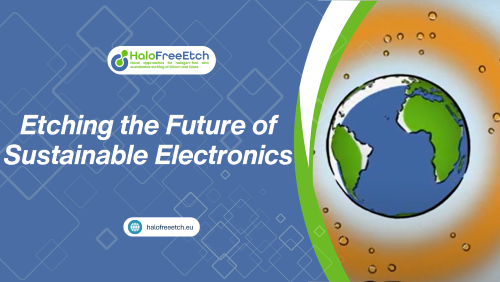
Shaping the Future of Microelectronics: Sustainable Innovation for a Greener Semiconductor Industry
We are proud to announce the publication of the first HaloFreeEtch newsletter, now available on our LinkedIn page.
The newsletter highlights our mission to revolutionize semiconductor manufacturing through halogen-free etching processes, fully aligned with the European Union’s vision for sustainable and responsible innovation. Readers will find insights on:
-
The project’s objectives and why they matter for the future of microelectronics
-
Innovative etching approaches that reduce chemical waste and environmental impact
-
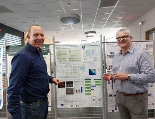
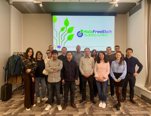
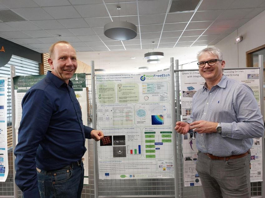
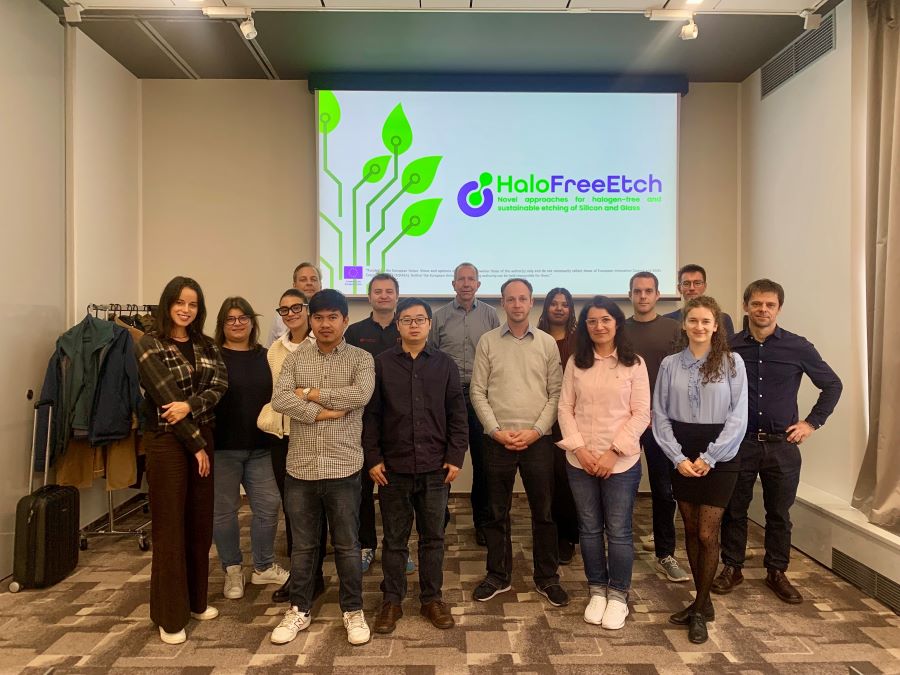
The strength of the HaloFreeEtch consortium, bringing together expertise from academia, research, and industry
-
Progress achieved in the first six months of the project
This is just the beginning of a series of newsletters where we will share project milestones, event highlights, scientific progress, and opportunities for engagement.
Don’t miss our updates! Subscribe to our newsletter and follow us on LinkedIn to stay informed about our journey towards a greener semiconductor industry.

